Looking for Custom Optical Components?
✔ OEM / ODM Customization
✔ Free Drawing DFM Technical Review
✔ 24-Hour Professional Quotation
✔ Flexible Low MOQ & Fast Prototypes
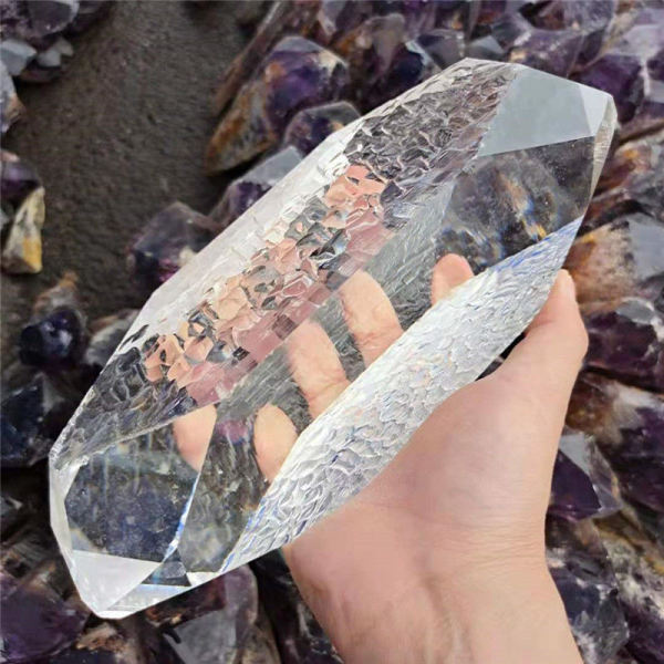
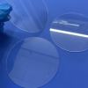
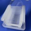
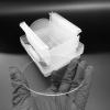
Quartz Wafer Manufacturer | Fused Silica Wafers for Semiconductor, Photolithography & UV Optics
| Share | |
|---|---|
| Categories | Custom Fused Quartz Windows |
| Brand | FELIX GLASS optical glass Manufacturing base |
| Model | FG-QT-005 |
| Material | High‑Purity Fused Silica (Amorphous SiO₂) |
| SiO₂ Purity | ≥99.99% |
| Diameter | 2″, 3″, 4″, 6″, 8″, 12″ (custom available) |
| Thickness | 0.1 mm – 5 mm (custom thickness) |
| TTV (Total Thickness Variation) | ≤5 μm (high precision ≤1 μm) |
| Surface Quality | 60/40, 40/20, 20/10 (MIL‑STD) |
| Surface Roughness (Ra) | ≤1 nm (DSP), ≤2 μm (lapped) |
| Optical Flatness | λ/2, λ/4, λ/10 @ 633 nm |
| Parallelism | <30 arcsec |
| Transmittance Range | 185 nm – 3500 nm |
| Average Transmittance | >90% |
| Thermal Expansion Coefficient | 5.5 × 10⁻⁷ /°C |
| Instant Temp Resistance | 1300°C |
| Available Finishes | DSP (double‑side polished), SSP (single‑side polished), lapped |
| Optional Features | Notch, flat edge, drilling, coating (AR/UV/IR) |
| FOB port | SHENGZHEN SHANGHAI GUANGZHOU |
| Terms of Payment | L/C, D/A, D/P, Western Union |
| Download |  |
Quartz Wafer Manufacturer | Fused Silica Wafers for Semiconductor & Optics
| Property | Value |
|---|---|
| Material | High‑Purity Fused Silica (Amorphous SiO₂) |
| SiO₂ Purity | ≥99.99% |
| Diameter | 2″, 3″, 4″, 6″, 8″, 12″ (custom available) |
| Thickness | 0.1 mm – 5 mm (custom thickness) |
| TTV (Total Thickness Variation) | ≤5 μm (high precision ≤1 μm) |
| Surface Quality | 60/40, 40/20, 20/10 (MIL‑STD) |
| Surface Roughness (Ra) | ≤1 nm (DSP), ≤2 μm (lapped) |
| Optical Flatness | λ/2, λ/4, λ/10 @ 633 nm |
| Parallelism | <30 arcsec |
| Transmittance Range | 185 nm – 3500 nm |
| Average Transmittance | >90% |
| Thermal Expansion Coefficient | 5.5 × 10⁻⁷ /°C |
| Continuous Working Temp | 1100°C |
| Instant Temp Resistance | 1300°C |
| Available Finishes | DSP (double‑side polished), SSP (single‑side polished), lapped |
| Optional Features | Notch, flat edge, drilling, coating (AR/UV/IR) |
Need Custom Optical Glass Solution?
Send us your drawing, dimension & coating requirements for fast quotation within 24 hours.
Get Free RFQ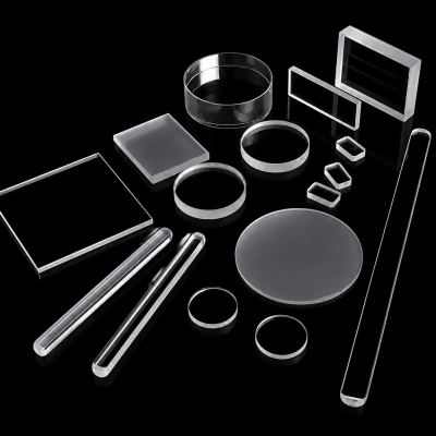
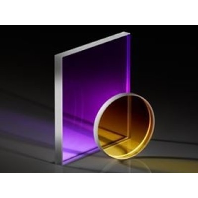
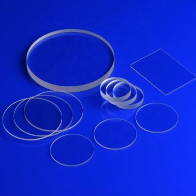
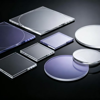
Custom Precision Optical & Glass Components Manufacturer – Felix Glass Co., Limited.
We supply Industrial Glass, Sapphire Optics, Optical Lenses/Prisms/Filters, Infrared IR Optics, Functional & Display Glass, N-BK7/H-K9L Optical Glass, supporting OEM mass production and laboratory custom prototypes. Flexible MOQ & free sample service available. Fill in the form to download full datasheets and get factory wholesale price within 24 hours.
- Name
- *Title
- *Content
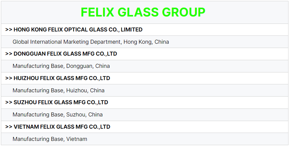

- What is the minimum order quantity for custom precision optical glass components?
FELIX OPTICAL GLASS offers highly flexible MOQs to support customer projects, including prototype testing, small-batch trial orders, and high-volume production. All products can be fully customized to your drawings, tolerances, and application standards. Please send us your specifications, and we will reply within 1-5 hours and provide an accurate quotation after careful evaluation within 1-2 days.
- Can I get free glass samples for testing before bulk order?
Yes, our FELIX GLASS factory supports sample testing for a wide range of precision optical glass components and assemblies. The lead time for sample production is 3 to 7 working days. Please contact us today to arrange samples and obtain a customized solution that meets your needs.
- What is the production lead time for custom optical glass components?
A: The production cycle for standard samples is 3-10 working days, while mass production requires 15-35 working days, depending on the complexity of the product and the order quantity. We provide reliable precision optical glass components and fast delivery services for orders from industries such as defense, industrial equipment, medical devices, shipbuilding, robotics, automotive, and aerospace. Please submit your project details so we can provide you with an accurate delivery schedule.
- Are your optical glass products ISO, CE and RoHS certified?
All precision optical glass components from FELIX OPTICAL GLASS comply with ISO quality system standards as well as CE and RoHS requirements. We provide comprehensive test reports, spectral graphs, material certificates, and inspection documents for customer review. Please feel free to request complete certification details and a formal quotation at any time.
- Do you offer one-stop custom optical glass processing services?
Yes. We offer a full range of precision optical glass component processing services, including CNC machining, precision grinding, optical polishing, chemical/physical tempering, vacuum coating (AR anti-reflective coating, AF anti-fingerprint coating, AG anti-glare coating, IR infrared coating), and screen printing. From raw materials to finished products, every step is completed in our own factory. Please tell us your needs, and we will provide you with the most cost-effective solution.
- Name
- *Title
- *Content
With 19 years of experience as a precision optical glass expert, we provide comprehensive and satisfactory customized solutions.
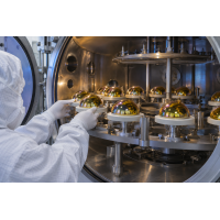 Felix Glass Expands IR Optics Production | Faster Lead Time for Custom ZnS, ZnSe, Sapphire & Fused Silica WindowsFelix Glass manufactures custom ZnS, ZnSe, sapphire domes & fused silica IR windows. Fast prototype and AR coating available. Get your technical quote within 24h for thermal imaging & laser systems.
 DMS Cover Glass Material Selection: Aluminosilicate vs Borosilicate Glass for In-Cabin CameraSelecting the right substrate impacts DMS camera lifespan & image quality. This guide compares aluminosilicate and borosilicate glass. Felix Glass provides both substrates with printing and coating.