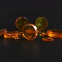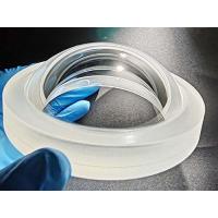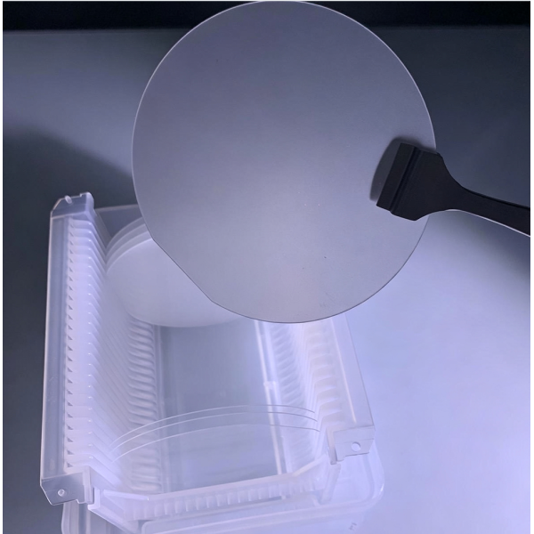
2.1 Full in‑house manufacturing workflow
Crystal growth → slicing → lapping → annealing → CMP polishing → clean‑room packaging, no intermediate outsourcing for stable quality control.

✔ OEM / ODM Customization
✔ Free Drawing DFM Technical Review
✔ 24-Hour Professional Quotation
✔ Flexible Low MOQ & Fast Prototypes
| Share | |
|---|---|
| Categories | Sapphire Optical Windows |
| Brand | FELIX GLASS optical glass Manufacturing base |
| Model | FG-CSOC-LD201 |
| Material | Single‑crystal α‑Al₂O₃ Sapphire, Purity ≥99.996% (In‑house crystal growth) |
| Available Diameter | 2",3",4",6",8", up to 12"(300mm), custom sizes supported |
| Crystal Orientation | C‑plane(0001), A‑plane(11‑20), M‑plane(10‑10), R‑plane(1‑102) |
| Surface Finish | SSP Single‑Side Polished / DSP Double‑Side Polished / Lapped / As‑Slic |
| TTV | 100μm‑2000μm, customizable |
| Roughness Ra | ≤0.5nm (Polished surface) |
| Manufacturing Process | Ingot growth → X‑ray orientation → Multi‑wire slicing → Lapping → Annealing → CMP polishing → Clean‑ |
| Packaging | Class‑100 clean wafer box, anti‑static packaging |
| Application | GaN epitaxy, LED, semiconductor RF device, aerospace IR window, deep‑sea ROV viewport, thin‑film dep |
| FOB port | SHENGZHEN SHANGHAI GUANGZHOU |
| Terms of Payment | L/C, D/A, D/P, Western Union, T/T |
| Download |  |
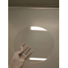
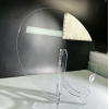
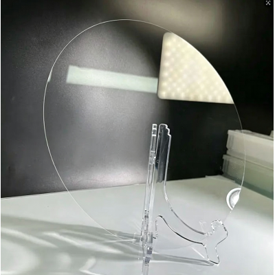
Hong Kong Felix Optical Glass Co., Limited delivers high‑quality custom precision sapphire wafers manufactured fully in‑house. Made from monocrystalline α‑Al₂O₃, these substrates support SSP / DSP polishing for GaN epitaxy, aerospace EO/IR, deep‑sea ROV, high‑temperature optical and semiconductor applications. Strict clean‑room production guarantees low TTV, high flatness and ultra‑low surface roughness for high‑yield epitaxial processing.
This product belongs to Custom Sapphire Optical Components, optimized for semiconductor and aerospace optical engineer search intent.
All parameters shown are typical reference values. Final dimension, crystal orientation, polishing grade and tolerance shall be confirmed by official engineering drawings and project specifications.
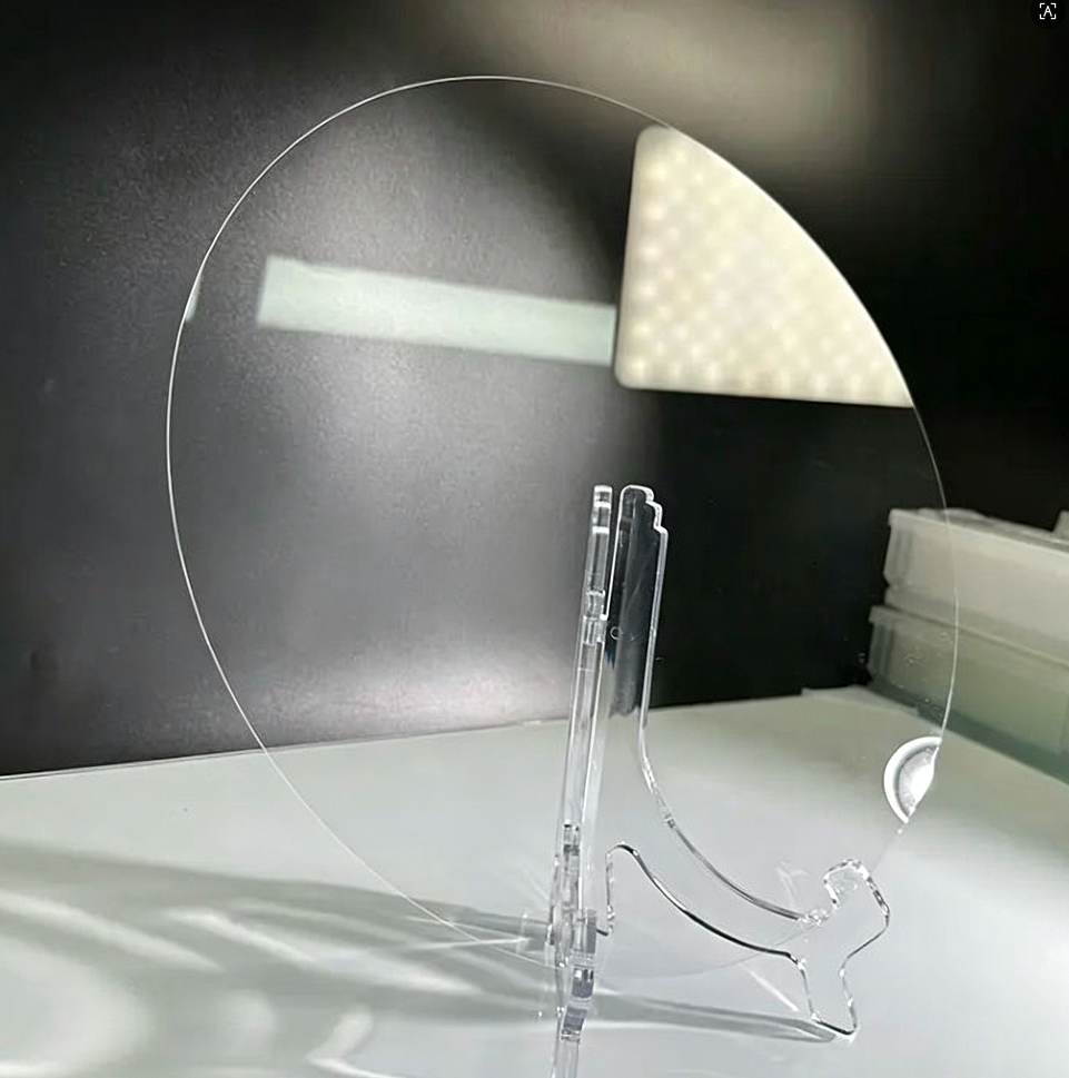
Our monocrystalline sapphire wafer series solves core engineering requirements for semiconductor epitaxy, aerospace and deep‑sea optical systems, delivering high flatness, low defect density and outstanding environmental stability.
Crystal growth → slicing → lapping → annealing → CMP polishing → clean‑room packaging, no intermediate outsourcing for stable quality control.
C‑plane, A‑plane, R‑plane, M‑plane to match LED, Micro‑LED, power‑semiconductor and optical‑grade application requirements.
Excellent high‑temperature, plasma and corrosion resistance for aerospace, deep‑sea and harsh industrial operating environments.
Explore more optical parts in Felix Glass product catalog.
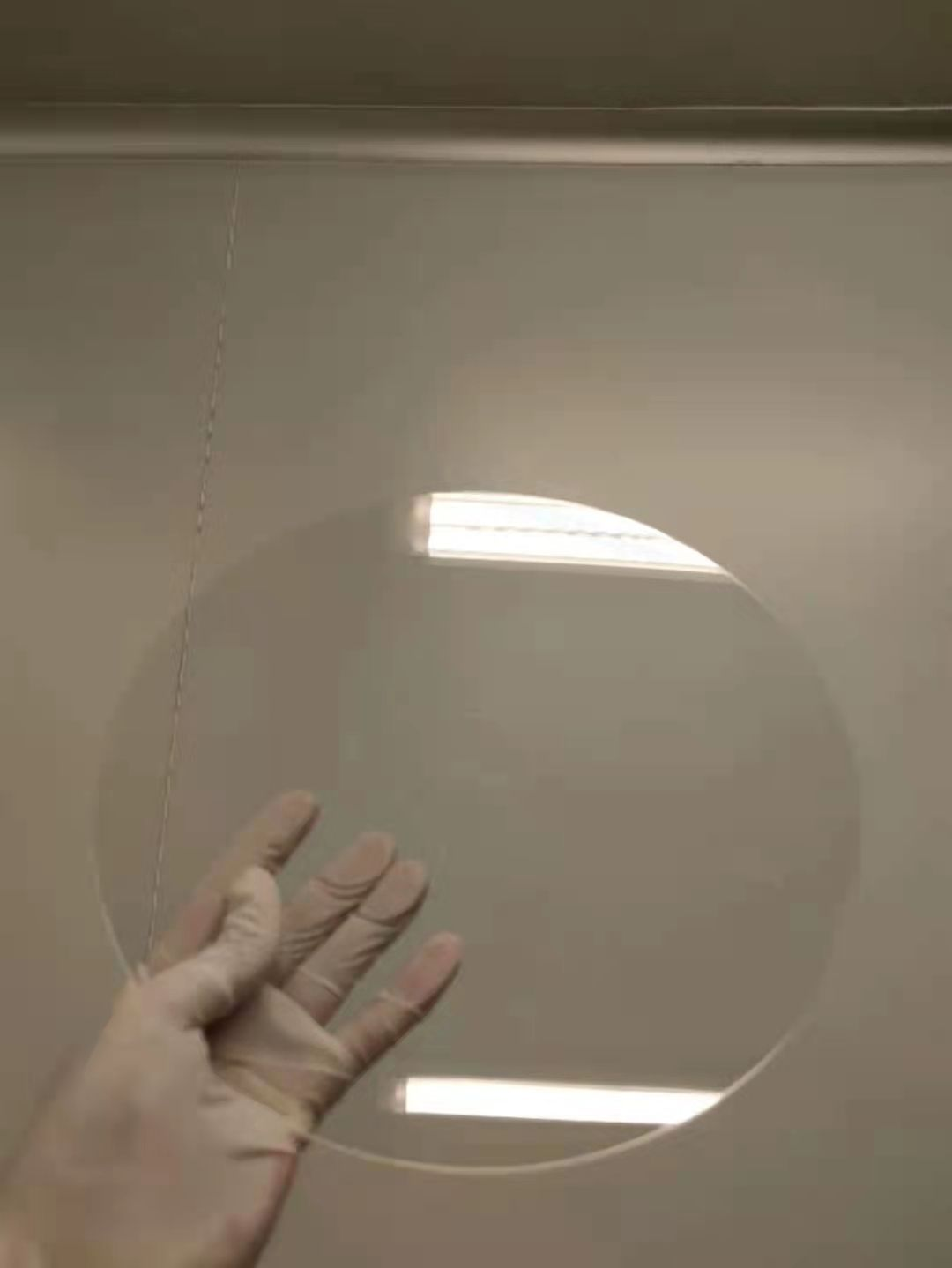
Monocrystalline α‑Al₂O₃ sapphire wafers are widely deployed across semiconductor epitaxy, aerospace optoelectronics and deep‑sea observation equipment.
TTV, bow, warp and surface roughness directly determine epitaxy yield. Submit drawing for manufacturability review.
Hong Kong Felix Optical Glass implements full‑chain control inside clean‑room facilities for large‑diameter sapphire wafer production.
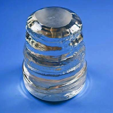
High‑quality monocrystalline α‑Al₂O₃ sapphire ingot preparation.
Precision wire‑saw slicing to target wafer thickness.
Surface lapping plus thermal annealing to eliminate slicing internal stress.
Rough/fine polishing, final CMP chemical‑mechanical polishing and RCA clean‑room cleaning.
View our manufacturing strength on About Us.
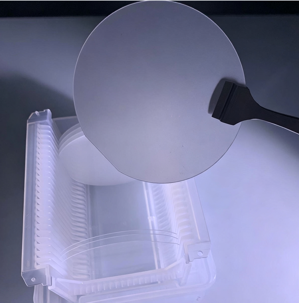
Large‑diameter sapphire wafers support multiple crystal planes and polishing grades for different semiconductor and optical projects.
Every wafer batch goes through TTV, bow, warp, surface roughness and defect inspection inside clean‑room before delivery. Customers can specify inspection standards according to epitaxy or optical design requirements.
Find more design suggestions in our technical blog.
Below lists common custom options. Our engineers will evaluate manufacturability after receiving your CAD drawings.
| Specification item | Available options | Project confirmation factor |
|---|---|---|
| Material | Single‑crystal α‑Al₂O₃ Sapphire | Optical / semiconductor application spectrum & operating environment |
| Available Diameter | 2",3",4",6",8", up to 12", custom sizes | Epitaxy equipment chuck size, assembly mechanical constraints |
| Thickness Range | 0.25 mm‑1.0 mm, custom thickness upon request | Wafer handling strength, device‑process requirements |
| Crystal Orientation | C‑plane (0001), A‑plane (11‑20), R‑plane (01‑12), M‑plane (10‑10) | Epitaxial film growth requirement, device design |
| Polishing Grade | SSP(Single‑Side Polished), DSP(Double‑Side Polished), Lapped | Epitaxy process, optical transmission demand |
| TTV | ≤10 μm (epitaxy grade, customizable) | Photolithography & epitaxy yield target |
| Surface Roughness Ra | ≤0.5 nm (CMP polished surface) | Epitaxy layer quality, scattering‑loss requirement |
| Notch / Flat Marking | Notch, primary flat, secondary flat, custom orientation mark | Wafer‑handling equipment compatibility |
| Packaging | Class‑100 clean‑room wafer carrier, vacuum sealed | Fab incoming‑particle‑control requirement |
After drawing review, crystal orientation and polishing specification confirmed, lead‑time reference as follows:
For epitaxy trial, optical performance and process verification.
Process validation before formal mass‑production.
Actual delivery depends on ingot blank stock, CMP capacity and clean‑room scheduling.
Class‑100 clean‑room wafer carrier + vacuum‑sealed export‑grade packaging, suitable for air freight to semiconductor fabs.
Below are typical performance descriptions. Real indicators must match project drawings and fab incoming‑inspection specification.
C‑plane (0001) is industry standard for GaN‑based LED / Micro‑LED epitaxy. Send your device specification for further consultation.
Yes, we support up to 12‑inch custom sapphire wafers. Please share your equipment chuck drawing for manufacturability evaluation.
We can provide TTV, bow‑warp, surface‑roughness inspection reports for each batch for fab incoming‑quality audit.
SSP: only working side CMP polished; DSP: both‑side CMP polished, better flatness for high‑end lithography‑related epitaxy process.
Yes, we support small‑batch R&D prototype for semiconductor research institutes and aerospace project teams.
Notch, primary‑flat and secondary‑flat orientation marking are available according your wafer‑handling equipment requirements.
Please provide target diameter, thickness, crystal orientation, polishing grade, notch/flat requirement and estimated quantity. Our optical‑semiconductor engineering team will return formal quotation and lead‑time within 24 working hours.
Send us your drawing, dimension & coating requirements for fast quotation within 24 hours.
Get Free RFQ
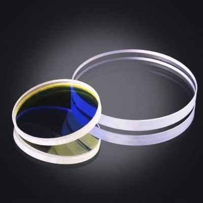
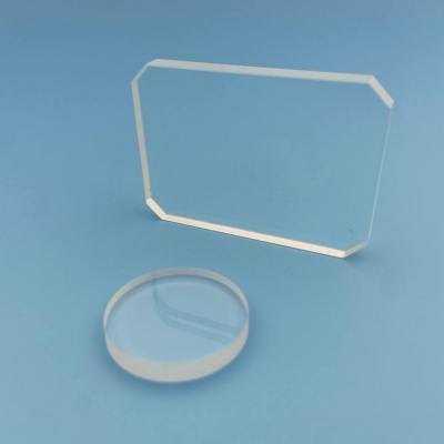
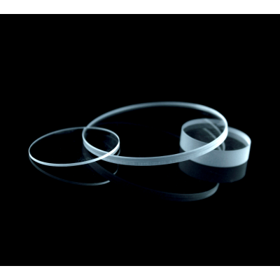
We supply Industrial Glass, Sapphire Optics, Optical Lenses/Prisms/Filters, Infrared IR Optics, Functional & Display Glass, N-BK7/H-K9L Optical Glass, supporting OEM mass production and laboratory custom prototypes. Flexible MOQ & free sample service available. Fill in the form to download full datasheets and get factory wholesale price within 24 hours.
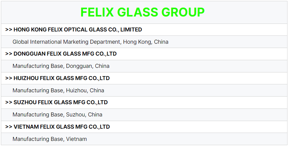

FELIX OPTICAL GLASS offers highly flexible MOQs to support customer projects, including prototype testing, small-batch trial orders, and high-volume production. All products can be fully customized to your drawings, tolerances, and application standards. Please send us your specifications, and we will reply within 1-5 hours and provide an accurate quotation after careful evaluation within 1-2 days.
Yes, our FELIX GLASS factory supports sample testing for a wide range of precision optical glass components and assemblies. The lead time for sample production is 3 to 7 working days. Please contact us today to arrange samples and obtain a customized solution that meets your needs.
A: The production cycle for standard samples is 3-10 working days, while mass production requires 15-35 working days, depending on the complexity of the product and the order quantity. We provide reliable precision optical glass components and fast delivery services for orders from industries such as defense, industrial equipment, medical devices, shipbuilding, robotics, automotive, and aerospace. Please submit your project details so we can provide you with an accurate delivery schedule.
All precision optical glass components from FELIX OPTICAL GLASS comply with ISO quality system standards as well as CE and RoHS requirements. We provide comprehensive test reports, spectral graphs, material certificates, and inspection documents for customer review. Please feel free to request complete certification details and a formal quotation at any time.
Yes. We offer a full range of precision optical glass component processing services, including CNC machining, precision grinding, optical polishing, chemical/physical tempering, vacuum coating (AR anti-reflective coating, AF anti-fingerprint coating, AG anti-glare coating, IR infrared coating), and screen printing. From raw materials to finished products, every step is completed in our own factory. Please tell us your needs, and we will provide you with the most cost-effective solution.