
Products · Custom ITO Conductive Glass
Patterned ITO Conductive Glass
Custom transparent electrode layouts, conductive tracks and isolation patterns
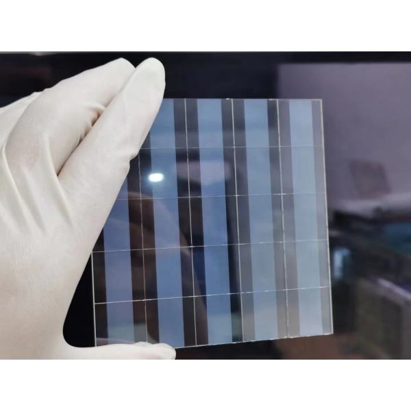
Custom patterned ITO glass with drawing-based electrodes, contact pads and isolation regions for sensing, research, optoelectronic and transparent heater projects.
View Pattern Specifications1. Custom Transparent Electrode Patterns
Felix Glass supports custom patterned ITO conductive glass projects built around customer drawings and electrode layouts. Selected regions of the indium tin oxide layer form conductive tracks, pads or active areas, while defined isolation regions separate electrical networks.
Submit your pattern artwork, substrate requirements and electrical targets for manufacturing review. The final pattern, process route and acceptance criteria are confirmed for the specific design and quantity.
2. Custom Specification Overview
| Parameter | Specification basis |
|---|---|
| Substrate | Soda-lime, borosilicate or fused silica grade subject to review |
| Glass geometry | Outline, thickness, holes, edges and tolerances to drawing |
| ITO pattern | Conductive regions, tracks, pads, isolation gaps and exclusions |
| Feature dimensions | Line width, gap width and registration tolerances reviewed from artwork |
| Sheet resistance | Target and uniformity of the retained ITO film in Ω/□ |
| Circuit resistance | Specified pad-to-pad resistance and continuity checks |
| Isolation | Resistance or leakage criterion under defined test conditions |
| Optical requirements | Transmission band, clear aperture, haze and pattern appearance |
| Contacts | ITO pads or additional contact structures by agreement |
| Documentation | Controlled artwork revision, inspection scope and lot records |
No single minimum feature size or resistance range applies to every substrate and pattern. Confirm achievable values after reviewing the full layout.
3. Define Conductive Regions and Isolation
Mark which regions retain ITO and which regions must be electrically isolated. Identify each electrical network, terminal and active area. A visible line in a drawing must be clearly classified as a conductor boundary, removed-film region or annotation.
Isolation is an electrical requirement as well as a geometric feature. A visually apparent gap can still contain residual conductive material. Specify acceptable resistance or leakage between networks, including test voltage, environment and measurement duration where relevant.
4. Select the Substrate and Coating Stack
Choose glass grade and thickness around the optical band, mechanical interfaces and downstream processing. Specify surface flatness, edge finish and any barrier layer when needed for device fabrication.
If other coatings, prints or adhesives are present, provide the layer sequence and face assignments. The patterning process must preserve the intended substrate and functional layers. A design qualified on one glass or coating stack is not automatically interchangeable with another.
5. Sheet Resistance vs. Track Resistance
Sheet resistance describes the retained conductive film. Track resistance also depends on path length, width, geometry and contacts. Specify both when the circuit function requires them.
For an ideal uniform rectangular strip with full-width contacts, R = RₛL/W. Bends, branching, narrowed regions, partial contacts and nonuniform film require a more appropriate model or measurement. Do not apply the simple relationship to a complex network without checking its assumptions.
Provide permitted pad-to-pad resistance and identify measurement points. This helps distinguish film variation from contact effects or pattern defects.
6. Line Width, Gap Width and Registration
Dimension critical line and gap widths with tolerances, and identify where they are measured. Include alignment marks, datum edges and any registration requirement relative to holes, printed artwork or subsequent layers.
Distinguish nominal artwork dimensions from required finished-feature dimensions. Patterning can alter edge profiles, so the inspection definition should describe the accepted final feature.
For repeated electrode arrays, specify pitch, spacing and any cumulative positioning limits. Avoid relying on an undimensioned image as the only manufacturing reference.
7. Patterning Route Selection
Industry approaches include photolithography with etching and laser-based film removal. The suitable route depends on material, film stack, pattern scale, edge requirements and quantity. Felix Glass reviews the proposed manufacturing scope against the drawing before quotation.
Evaluate the resulting electrical isolation, conductor continuity, edge condition, residues and substrate effects. A process name alone does not guarantee a particular resolution or optical finish.
If the process is mandated for your device, identify that requirement and its reason. Otherwise, provide measurable acceptance criteria so a suitable route can be proposed.
8. Optical Transmission and Pattern Visibility
Specify transmission across the required spectral band and state whether measurements apply to a retained-ITO region, an uncoated region or the complete functional aperture. An aperture-average result can conceal local differences.
ITO-covered and cleared regions can have different reflection or color. If the pattern lies over a display or imaging area, define viewing conditions and acceptable visibility, haze or scatter.
For optical sensing, include illumination wavelength, viewing angles and any imaging-quality limits. Visible clarity does not by itself establish ultraviolet or near-infrared performance.
9. Pads, Busbars and Connections
Provide pad dimensions, locations, contact method and any required additional metallization. Keep contact zones separate from the optical aperture and from areas reserved for bonding or sealing.
Specify contact resistance and attachment requirements where relevant. Probe or connector forces, thermal exposure and adhesive chemistry can affect contact reliability.
Confirm whether the order covers patterned glass alone or also includes busbars, deposited contact layers, attached leads or other assembly work. ITO pads should not be assumed to accept every soldering or bonding process.
10. Typical Development Applications
| Application | Pattern function | Key validation |
|---|---|---|
| Optoelectronic research | Defined transparent electrode areas | Alignment, contacts and device-stack compatibility |
| Sensing structures | Separate electrodes and signal paths | Isolation, active area and environmental response |
| Touch-interface development | Transparent electrode networks | Controller compatibility and complete sensor performance |
| Transparent heaters | Controlled current paths and heating zones | Resistance, power distribution and mounted temperature map |
| Laboratory electrochemistry | Defined conductive regions | Exposed area, electrolyte compatibility and contact protection |
Patterned ITO glass is a component rather than a complete sensor, display or controlled heater. Performance must be validated with the intended electronics and assembly.
11. Process Compatibility and Handling
Describe downstream deposition, cleaning, annealing, bonding and chemical exposure. Include temperature, atmosphere, time and repeated-cycle requirements where they affect electrical or optical performance.
Treat the exposed film and contact areas as functional surfaces. Specify acceptable handling locations and cleanliness needs. A cleaning or surface-treatment procedure should be validated for the complete stack rather than assumed compatible with every ITO product.
If performance after processing matters, include post-process continuity, isolation, resistance and optical checks in the qualification plan.
12. Inspection and Electrical Acceptance
Agree on dimensional inspection of critical features, visual checks of pattern edges and electrical testing of designated networks. Identify open circuits, unintended bridges and local damage as applicable defect categories.
| Characteristic | Acceptance definition |
|---|---|
| Film sheet resistance | Method, locations, temperature and allowed variation |
| Track resistance | Terminal pair, contact arrangement and permitted range |
| Isolation | Network pair, voltage, leakage or resistance limit and environment |
| Pattern dimensions | Feature limits, datums and registration rules |
| Optical quality | Spectral band, measured region and appearance conditions |
Define sampling and reporting requirements. Flat witness-coupon data can support film control but do not replace electrical verification of the finished pattern where it is required.
13. Artwork, Prototypes and Production RFQ
Provide a dimensioned PDF and editable vector or CAD artwork in an agreed format, such as DXF. Include units, scale, layer names, pattern polarity, viewing side, orientation and revision. Explicitly state whether the artwork is viewed from the coated face to prevent mirrored production.
Label every network and supply a test-point map or connection table where useful. State prototype and production quantities, substrate specifications, coating targets, contact requirements and inspection documentation.
Prototype approval should cover final dimensions, electrical behavior and optical appearance. Confirm tooling or setup costs, packaging, delivery schedule and change-control requirements before production release.
14. Frequently Asked Questions
What is patterned ITO conductive glass?
It is glass with defined conductive ITO regions and isolation areas that form a specified electrode or circuit layout.
Can I send a picture of the pattern?
A picture helps explain intent, but production normally requires controlled dimensions and editable artwork with units and orientation.
What minimum line width can you supply?
It depends on the substrate, coating, process and acceptance requirements. Submit the layout for project-specific confirmation.
Does a visible gap guarantee electrical isolation?
No. Define an electrical isolation test because residual film or contamination can create leakage or bridges.
Is sheet resistance enough to specify my circuit?
Not always. Complex patterns also need terminal resistance, continuity and isolation requirements.
Can the pattern be used as a heater?
Potentially. Current distribution, contacts, power and mounted thermal performance must be designed and validated.
Can contacts or leads be included?
They can be reviewed as a separate part of the supply scope. Specify the attachment method and reliability requirements.
How do I prevent a mirrored pattern?
Identify the coated face and viewing direction on both the drawing and artwork, and include an asymmetric orientation feature where appropriate.
15. Request a Patterned ITO Glass Quote
Send your drawing, pattern artwork and electrical requirements to Felix Glass. Include substrate grade, dimensions, transmission band, sheet resistance, critical line and gap dimensions, test-point map and quantities.
Dongguan Felix Glass Co., Ltd.
Email: james@felixglass.com