Semiconductor Optical Components: Materials & Precision Manufacturing Guide
Semiconductor manufacturing equipment relies on ultra-precision optical systems to support wafer inspection, lithography alignment, metrology measurement, and plasma processing monitoring. These optical subsystems require nanometer-level precision, and even minor optical distortion can directly impact chip yield and overall production accuracy.
As semiconductor process nodes continue to shrink, optical components must achieve superior transmission stability, extreme surface precision, and contamination-free performance under high-energy radiation and vacuum operating environments.
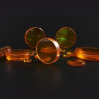
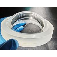
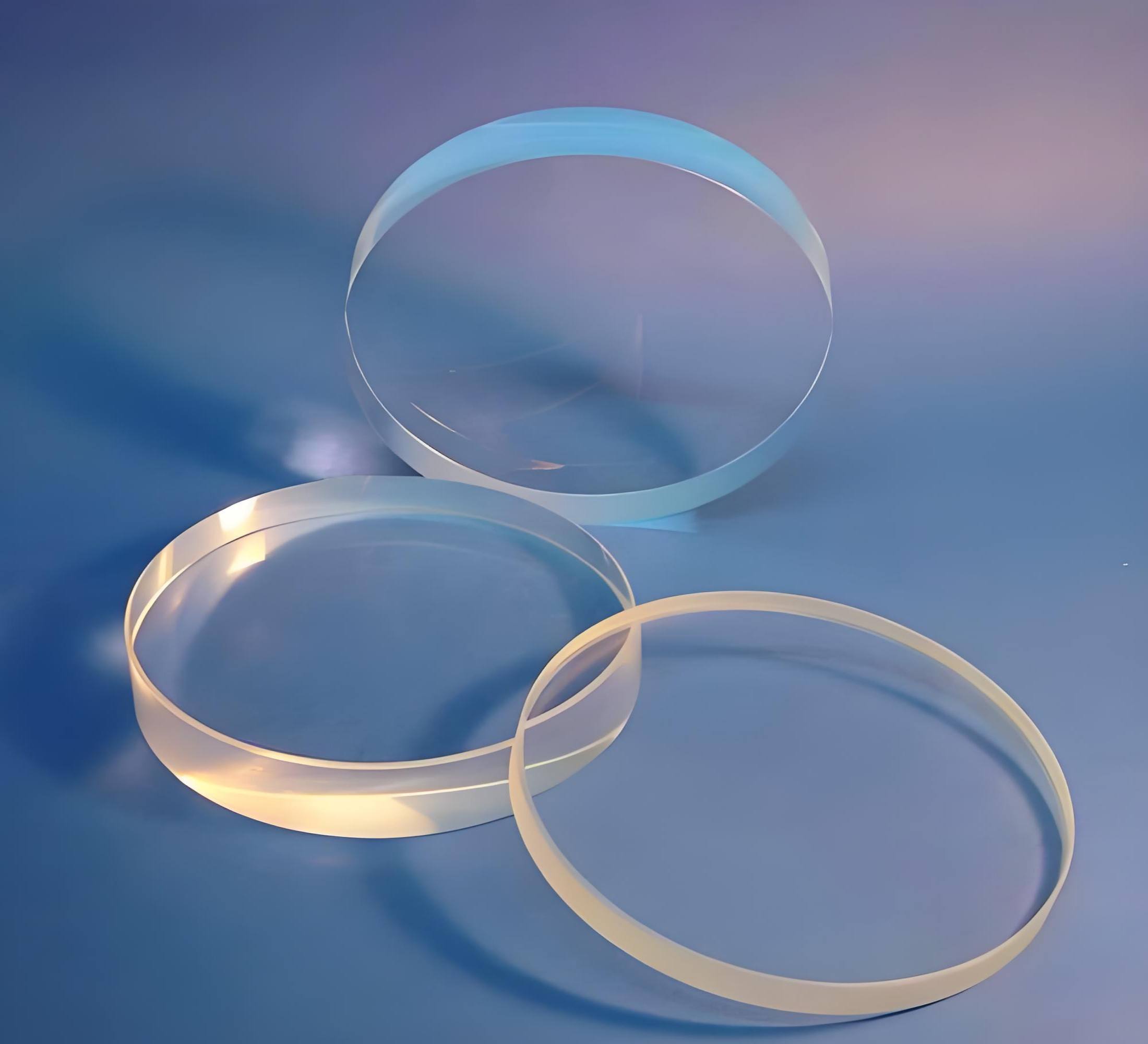
Felix Glass specializes in custom manufacturing high-precision optical components for semiconductor equipment. Our product portfolio covers quartz glass windows, fused silica optics, optical lenses, precision filters, and tailor-made UV & IR optical substrates, serving semiconductor OEMs and equipment integrators worldwide.
1. Core Role of Semiconductor Optical Systems
Optical components act as vital core subsystems inside wafer fabrication equipment. They enable high-precision imaging, position alignment and micro/nano-scale dimensional measurement. The performance of these optics fundamentally determines accuracy in lithography projection, wafer defect detection and real-time plasma process monitoring.
2. Key Technical Challenges in Semiconductor Optical Applications
Optical engineers and equipment manufacturers face multiple strict technical barriers inside semiconductor fabrication facilities:
- Nanometer-level precision standard required for wafer inspection and lithography alignment
- Degradation risk of optical materials under continuous high-energy plasma and UV irradiation
- Extreme sensitivity to particle contamination within vacuum and cleanroom environments
- Thermal deformation risks during long-duration high-power operation
- Demanding flatness and surface accuracy standards for optical base substrates
3. Essential Technical Specifications for Semiconductor-Grade Optics
To adapt to harsh fab working conditions, qualified semiconductor optical parts need to satisfy the following requirements:
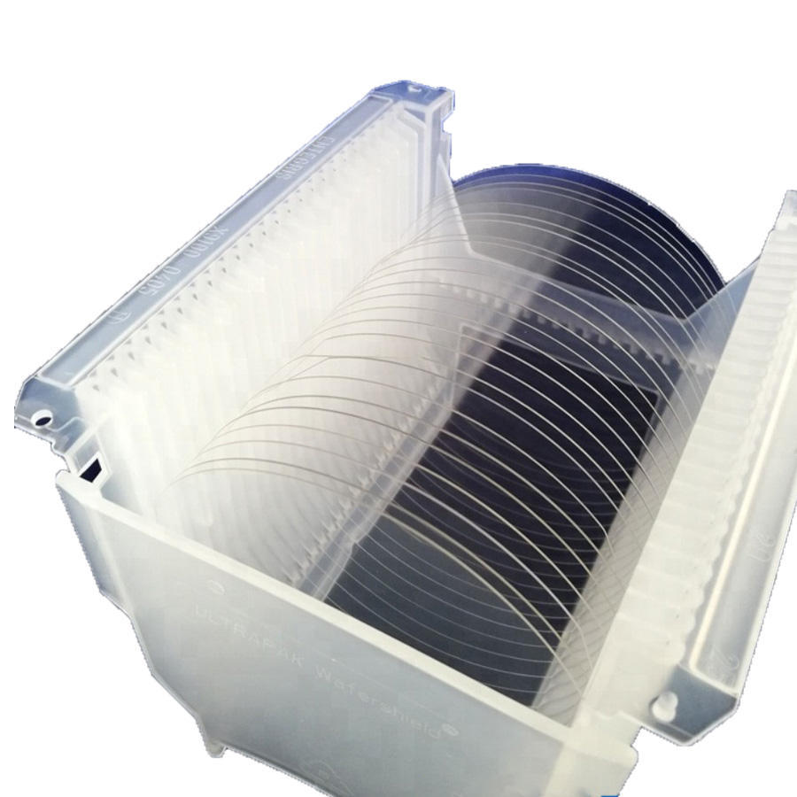
- Ultra-high surface accuracy up to λ/20 for critical lithography optical elements
- Ultra-low surface roughness, reaching <1 nm RMS for high-end precision optics
- Stable high transmittance covering UV, deep UV (DUV) and visible light wavebands
- Reliable thermal stability under prolonged continuous exposure
- Strictly particle-free, contamination-controlled optical surfaces
- High laser damage threshold to adapt to high-energy beam systems
4. Critical Factors to Evaluate When Sourcing Optical Components
Professional optical engineers assess multiple indicators before confirming suppliers for semiconductor optics:
- Applicable wavelength spectrum (DUV / EUV / UV / visible / IR, matched to production processes)
- Cleanroom compatibility and contamination control standards
- Flatness and surface figure accuracy tolerances
- Matching thermal expansion coefficient with mechanical structural parts
- Resistance against plasma corrosion, ultraviolet radiation and chemical erosion
- Full compliance with industry semiconductor equipment manufacturing standards
5. Custom Optical Products for Semiconductor Industry
Felix Glass delivers diversified precision optical components tailored for wafer manufacturing equipment:
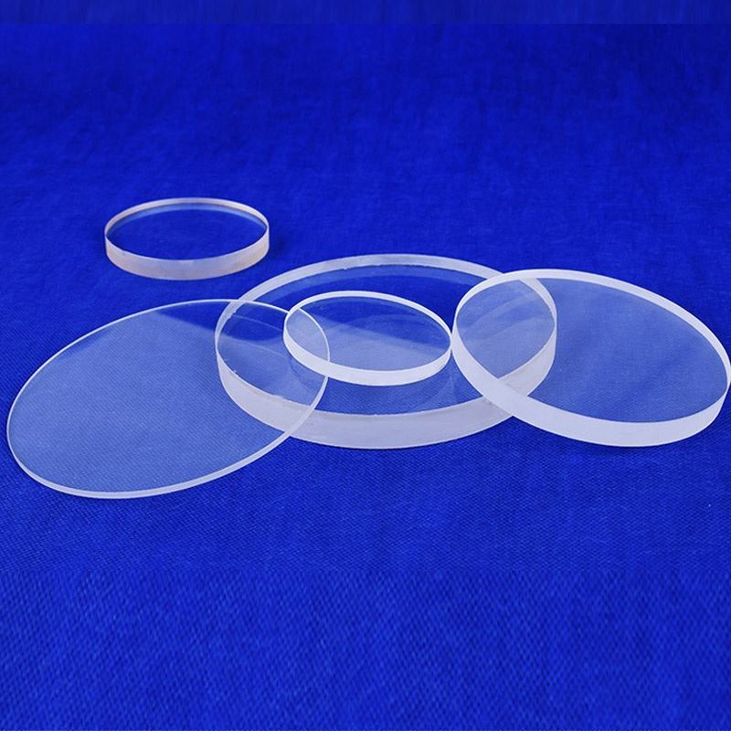
- Fused Silica Optical Windows
- High Purity Quartz Glass Components
- UV Transmitting Optical Lenses
- Precision Optical Filters
- Ultra High Flatness Optical Windows
- Infrared Optical Components for Process Monitoring Systems
6. Optical Material Guide & Typical Application Scenarios
Material selection depends on optical precision demands and the operating environment inside semiconductor production lines:
- Fused Silica: Ideal for high-purity UV and DUV lithography systems, featuring ultra-low thermal distortion
- Quartz Glass: Widely adopted for wafer inspection equipment with excellent thermal and chemical stability
- Sapphire: Robust optical windows for plasma equipment and other harsh working environments
- Calcium Fluoride (CaF₂): Preferred material for UV lithography requiring outstanding deep UV transmittance
- BK7 Optical Glass: Suitable for visible-light metrology and optical alignment systems
7. Complete In-House Manufacturing Capabilities
We implement full-process independent production to guarantee stable quality for semiconductor optical components:
- Ultra-precision CNC machining for high-flatness optical substrates
- Sub-nanometer surface polishing for lithography-grade optical surfaces
- Custom UV-grade and DUV-grade optical coating services
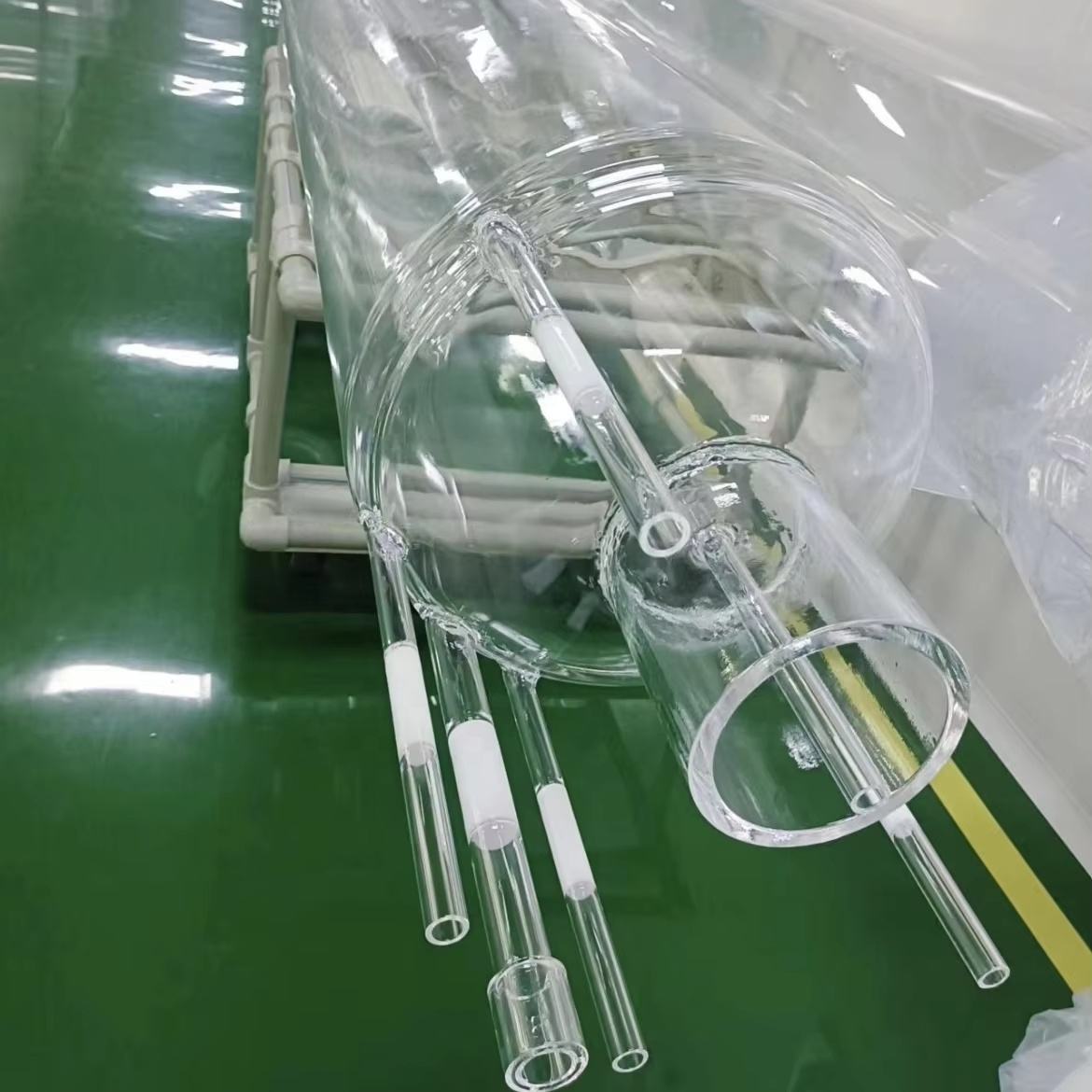
- Laser cutting and precision edge finishing for quartz and fused silica workpieces
- Production supported under ISO Class 5–7 cleanroom standards
- Interferometer-based flatness testing and comprehensive surface defect inspection
8. Quality Control Standards & Industry Compliance
- Optical processing fully compliant with ISO 10110 optical drawing specifications
- Complete validation of cleanroom contamination control workflows
- Particle cleaning and particle-free inspection before every shipment
- RoHS and REACH certification to satisfy semiconductor equipment integration requirements
- Complete batch traceability for all quartz and fused silica optical products
- 100% surface defect detection via interferometric testing systems
9. Standard Optical Performance Parameters
Below are typical technical specifications for our semiconductor optical products:
- Transmission spectrum: 190 nm – 2500 nm (varies according to raw material)
- Surface accuracy: up to λ/20 for lithography-level optical elements
- Surface quality: 10-5 / 20-10 scratch-dig standard
- Flatness tolerance: ≤ λ/10 for precision alignment optical windows
- Surface roughness: <1 nm RMS for high-end customized optics
- Fused silica series features ultra-low thermal expansion coefficient
10. Main Application Fields of Semiconductor Optics
Our optical components are widely integrated into mainstream semiconductor manufacturing and testing equipment:
- Wafer lithography projection systems
- Wafer surface inspection and defect detection equipment
- Plasma etching real-time monitoring systems
- Metrology equipment and optical alignment devices
- UV laser semiconductor processing equipment
The performance of every optical component directly determines wafer yield, alignment precision and nanoscale manufacturing reliability.

11. Why Cooperate With Felix Glass for Semiconductor Optics
Our vertically integrated manufacturing system brings clear advantages for semiconductor equipment partners:
- Ultra-precision optical processing for lithography and wafer inspection systems
- Reliable and stable supply chain of high-purity fused silica and quartz raw materials
- Fast prototyping service for semiconductor equipment OEM projects
- Contamination-controlled production for cleanroom-grade optical components
- Optimized cost control via full in-house production workflow
12. Frequently Asked Questions
Q: Are you able to produce ultra-flat quartz windows used for wafer inspection equipment?
A: Yes. We manufacture high-flatness quartz and fused silica windows with sub-micron precision for all kinds of semiconductor inspection equipment.
Q: Can you provide optical components working under UV and deep UV wavebands?
A: Absolutely. We supply fused silica and CaF₂ optical elements specially designed for UV and DUV lithography systems.
Q: Can your optical products meet cleanroom-level application requirements?
A: All semiconductor optical components are manufactured under ISO Class 5–7 cleanroom production environments.
Q: Do you accept customized optical parts for lithography equipment?
A: We provide fully customized optical solutions to match unique demands of semiconductor equipment OEMs.
13. Submit Your Technical RFQ
If you need a formal technical quotation for semiconductor optical components, kindly prepare the following information:
- Engineering drawings or detailed optical specification sheet
- Working wavelength range (DUV / UV / visible / IR)
- Required flatness and surface accuracy tolerance
- Cleanroom grade requirements
- Order volume (prototype trial or mass production)
Our professional engineering team will complete technical assessment and send you the quotation within 24–48 hours.
Need Custom Semiconductor Optical Components?
Share your drawings, wavelength requirements & precision specs. Get professional engineering evaluation and competitive OEM quotation.
Request Free Technical Quote